TXtelsig YP552228 Wifi RF Amplifier
The YP552228 is a 2-stage 4.9-5.9GHz high efficiency, high linearity power amplifier based on InGaP/GaAs HBT technology. The amplifier provides a typical gain of 22 dB and P1dB power of 30.5 dBm, typical bias condition is 5.5V at 240 mA. The input and output are internally matched to 50Ω and require a minimum of external matching components to cover the entire 4.9GHz to 5.9GHz. The YP552228 is assembled in a 16-pin, 4mm×4mm, QFN package.
Features:
■4.9~5.9GHz Frequency Range
■3.3V~5.5V Operation
■3.0% EVM@24dBm for 802.11a 54Mbps, 5.5V
■3.0% EVM@22.5dBm for 802.11a 54Mbps, 5V
■2.5% EVM@18dBm for 802.11a 54Mbps, 3.3V
■240mA Quiescent Current
■22dB Gain (Typ)
■>20dB Input Return Loss@5.8GHz
■On-Chip Power Detector
Ordering Information
■YP552228 5.8GHz Linear Power Amplifier
■YP552228EVB-1 5.2GHz to 5.8GHz Evaluation PCB
■YP552228EVB-2 5.6GHz to 5.9GHz Evaluation PCB
Applications
■ IEEE 802.11a/n WLAN
■ IEEE 802.16 WiMax
■ 5.8GHz RFID
■ Spread-Spectrum and MMDS Systems
Aution! ESD sensitive device:
ESD Rating: Class1C
Value: Passes≥1000V min.
Test: Human Body Model (HBM) Standard: JEDEC Standard JESD22-A114
ESD Rating: Class IV
Value: Passes ≥1000V min.
Test: Charged Device Model (CDM) Standard: JEDEC Standard JESD22-C101
MSL Rating: Level 3 at +260 °C convection reflow
Standard: JEDEC Standard J-STD-020
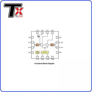
| Pin Description |
| Pin No. | Symbol | Description |
| 1, 4, 8, 9, 12 | NC/GND | No connection or Ground connection |
| 2, 3 | RF IN | RF input |
| 5 | VCTR | Power on/off control voltage |
| 6 | VBIAS | Bias voltage |
| 7 | VCCB | Supply voltage for bias |
| 10, 11 | RF OUT | RF output |
| 13 / 14 | VCC2 / VCC1 | Supply voltage for the 2nd / 1st stage |
| 15 | DET | Provides an output voltage proportional to the RF level |
| 16 | VCCD | Supply voltage for power detector |
| Pkg Base | GND | Ground connection |
| Absolute Maximum Ratings |
| Parameter | Rating | Unit |
| Input RF Power | 15 | dBm |
| Supply Voltage | -0.5 to +7.0 | V |
| Bias Voltage | -0.5 to +4.0 | V |
| DC Supply Current | 1000 | mA |
| Operating Ambient | | °C |
| Temperature | -40 to +85 |
| Storage Temperature | -40 to +150 | °C |